Coated samples are required in the field of electron microscopy to enable or enhance imaging of the sample. The creation of a metal sample on the conductive layer inhibits charging, reduces thermal damage, and improves the secondary electrical signal required for inspection of the terrain in the SEM. The fine carbon layer, ie the transparent electron beam, but the conductivity, required for X-ray microanalysis, supports a backup copy of the TEM image of the film on the grid. The resolution and application depend on the coating technology used.
Scanning electron microscopy imaging before painting
Limited or non-conductive material samples (ceramic, polymer, etc.), carbon and/or metal coatings. Low temperature samples were frozen and fractured, coated metals (Leica EM ACE600 frozen fracture and Leica EM VCT100) and low temperature SEM imaging.
TEM imaging is required before painting
Covering the Forva TEM grid needs to be coated with carbon that is electrically conductive. Grid glow discharge processing solutions that would otherwise fail to persist and be distributed to the grid. Frozen fracture samples were coated at low angles with metal and then replicas produced by carbon backup membranes (Leica EM ACE600 cryo-fracture and Leica EM VCT100 or LeicaEM BAF060) were imaged in TEM.
Sputter coating
The SEM of the sputter coating uses ultra-thin coated conductive metals such as gold/palladium (gold/palladium), platinum (Pt), gold (Au), silver (Ag), chromium (Cr) or铱 (Ir), to non-conducting or poorly conducting samples. Sputter coating prevents specimens from charging, otherwise it will occur because of the accumulated electrostatic field. This also increases the amount of secondary electrons that can be detected from the surface of the sample in the scanning electron microscope, thus increasing the signal-to-noise ratio. Sputtered films for SEM typically have a thickness in the range of 2-20 nanometers.
Benefits of SEM samples Sputtered metal:
Streamlined microscope damage
Increase heat transfer
Reduced sample charge (increased conduction)
Improved secondary electron emission
Improved edge resolution reduces beam penetration
Protection beam sensitive specimen
Carbon coating
It is widely used for the thermal evaporation of carbon for the preparation of electron microscope specimens. A carbon source - either in the form of a thread or rod is installed between two high current electrical terminals in a vacuum system. When the carbon source is heated to its evaporation temperature, a trickle of carbon is deposited onto the sample. The main application of carbon coating is EM electron microscopy, X-ray microscopy and support film for specimen (TEM) grid.
Electron beam coating
Both metals and carbon can vanish. The best electron beam coating layer is given, which is a very oriented process with a limited surface coating area. The electrons are focused on the target and heated and further evaporated. Charged particles are removed from the bundle. Therefore, a very low charged beam hits the sample. The heat is reduced and the effect of charged particles on the sample is reduced. Only a few runs are possible, then the source is reloaded and cleaned up. In general, an electron beam is used to coat in either direction is necessary (shadow and copy) or layer fine.
Introduction of refrigeration technology
Frozen fracture involves a series of techniques that reveal and replicate the internal components of the organelle and other membrane structures under an electron microscope. The ice from the freeze-etched removal layer passes through the sublimation and reveals the initially hidden film surface.
Freeze drying, also known as freeze drying, removes water from the frozen sample under high vacuum (sublimation). The result: a dry, stable sample that can be imaged under an electron microscope.
application
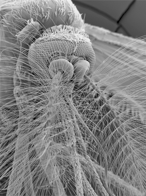
Figure 1: Mosquito antenna (courtesy, Dr. Daniela Gruber, Vienna, Austria)
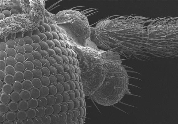
Figure 2: Drosophila Eyes (by Jin Lunxin, Leica Microsystems, Application Specialist)
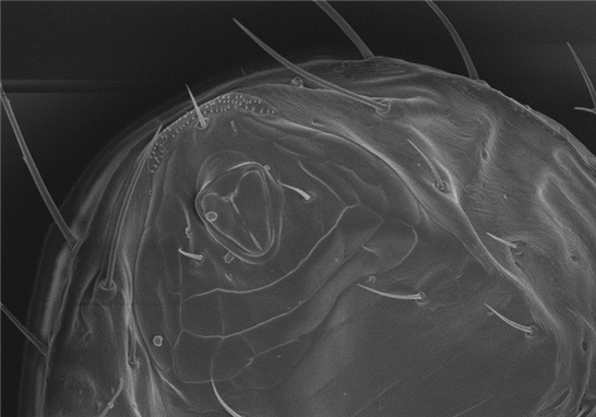
Figure 3: Red Spider (by Jin Lunxin, Leica Microsystems, Application Specialist)
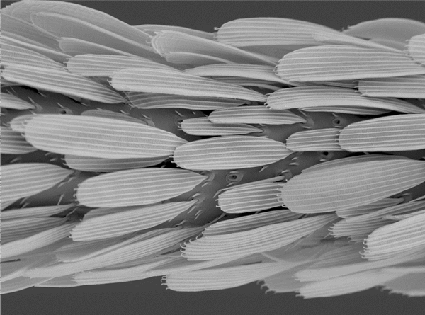
Figure 4: Mosquito legs (courtesy, core facility for cell imaging and ultrastructural research at the University of Vienna, Austria, Dr. Daniela Gruber)
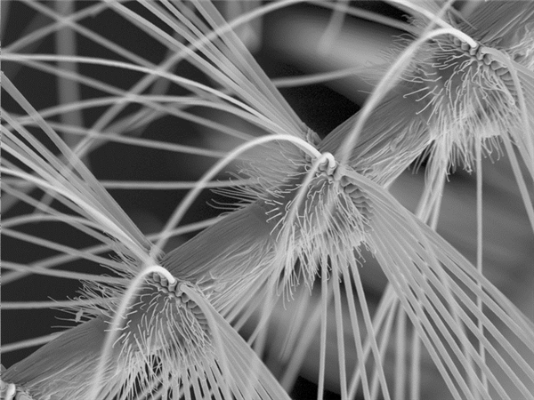
Figure 5: Antenna details (Dr. Daniel Gruber, core facility for cell imaging and ultrastructural research at the University of Vienna, Austria)
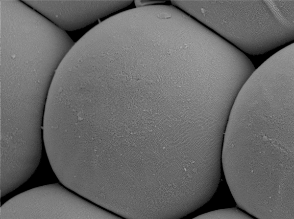
Figure 6: Mosquitoes in Ommatidien (Center for Cell Imaging and Ultrastructural Research at the University of Vienna, Courtesy Dr. Daniela Gruber, Austria)
Multifunctional Diaper Bags are becoming more and more popular as regular items for babies and parents. Whether it is a long-distance travel or a short trip, the Mummy Bag provides important convenience for babies and parents. The popularity of mommy bags has caused new parents to pay attention to infant travel, not only psychologically but also physical changes, with great significance.
Mini Diaper Bag,Mini Baby Bag,Mummy Bag For Travel,Multifunctional Diaper Bag
JOYBABIES PRODUCT CO.,LTD. , https://www.joybabiesproducts.com