5, DEK latest screen printing in a single trip to produce a variety of glue height
DEK introduced the latest addition screen technology, which allows users to generate multiple high-strength dots in a single printing stroke, thereby increasing throughput, reducing process steps, and improving equipment utilization. DEK's solution for generating a variety of spot heights also extends the useful life of scrapers or enclosed print head wipers and screens.
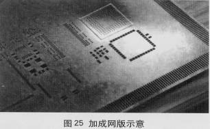
Add screen version see Figure 25.
Addition screen technology can be used on any side of the screen to perform addition operations on selected areas of the screen surface. Compared with the nominal height determined by the main screen thickness, the height of the spot in the selected area can be increased by 10 to 100 μm. Can also be added in any area of ​​the screen build, the largest surface area up to 40mm × 40mm, to meet customer requirements.
DEK's additive screen technology is implemented through precision processes that precisely control the increment of screen thickness within a specific range. It also allows DEK screen designers to trim and smooth the edges of the raised areas, making metal scrapers or closed printing. The wiper of the head (such as DEK's ProFlow transfer head, etc.) can easily slide up and down. This can extend the life of the squeegee or wiper and the screen, and improve its process control and repeatability.
DEK's new technology is suitable for applications that used to use more than one screen in the past, or when the solder paste needs to be changed, and can be applied to different components such as edge connectors.
The add-on screen manufacturing tolerances are as follows:
The minimum distance between two glue spots is ±0.5mm:
The maximum area is 40mm x 40mm:
Thickness tolerance is ±0.012mm;
The maximum glue spot thickness is 0.075mm.
6, DEK electroforming screen and variable height technology (VAHT)
DEK, a world-leading supplier of high-precision bulk extrusion printing solutions, once again made breakthroughs in the field of screen printing technology. Through its manufacturing process, combined with proprietary precision mesh height control methods, the electroforming screen printing technology was upgraded to a new level. .
The electroforming screen process is technically referred to as the "addition process," and the electroforming screen is "growthed" by electroplating the electroplated material onto the mandrel. The plating material is usually nickel, the mandrels are provided with a pattern of open, negative, photoresist images. This process produces a very precise, well-walled opening with a natural and also taper required for screen printing without the need for an additional finishing process. This very precise process produces an electroformed screen suitable for ultra-fine-pitch applications.
Electroforming screen features:
Electroforming screen is made of nickel atoms deposited on the surface of a layer of conductive tire mold. The fetal film has been covered with a positive (or grid) positive image formed by photosensitive resist;
〉 The mesh size is precise, the hole wall is smooth, and the trapezoidal cross section is conducive to solder paste printing;
〉 Unmatched tensile strength and hardness, extending screen life;
〉 It is very effective for printing large-area, fine-pitch components on printed circuit boards. Provides excellent printing performance for small BGA, UBGA, ultra-precision QFP and small chip components such as 0201.
DEK's Eform electroforming screen (hereafter referred to as DEKEform) screen provides excellent printing performance and ensures that the solder paste can closely contact the pad, apply it precisely to the pad, and deposit it on the pad with a higher percentage of solder paste . The reaction force generated by the DEKEform screen can achieve even distribution of the solder paste and make the solder paste cleanly away from the mesh. This technology also provides ultimate control over screen thickness and print uniformity. Guarantee the consistency of solder paste coating in precision spacing printing applications. Moreover, as the electronics industry is increasingly moving toward lead-free production and leadless printing. DEKEform Screens will be an indispensable tool for improving the release properties of solder pastes when printing more challenging lead-free solder pastes.
DEK's Eform screen process, combined with its innovative Variable Mesh Height Technology (VAHT), will enhance functionality. The coplanarity of printed circuit boards is a very common problem in the industry. Printed circuit boards and screen boards cannot be in close contact with each other because of the different heights of printed circuit boards. . VAHT is an intrinsic feature of DEKEform screens. The height of the bottom of the screen can be adjusted so that uniform and uniform sealing contacts are formed on the entire printed circuit board surface. The combination of Eform Screen and VAHT's two powerful technologies will bring superior solder paste printing results.
The screens produced by DEK's Dform process and inherent VAHT technology will be the perfect implementation technology for next-generation precision pitch SMT and semiconductor packaging technologies. As the boundaries of complex SMT assembly and semiconductor packaging processes become more and more blurred, the market's demand for advanced screen technology is increasingly evident.
In the field of electronic screen printing technology, in order to meet the needs of special printing, a variety of distinctive screens have come into being. Here is a brief introduction.
PDP (Plasmadisplay) screen
Developed specifically for Plasma Plasma Displays (PDPs), the screens are developed with composite screen technology, high tension, and print reproducibility.
〉 HS very thin screen version - the challenge of screen printing limit.
HS Super thin-gauge wire mesh (HS Super), together with a company's exclusive development of ultra-high resolution emulsion (SRX-M), and the most advanced parallel exposure device, make the fine pattern fine pattern and Printing reached its highest level.
〉 MS Metal Plate - High Precision S/S Network + Metal Film
The MS Metal Plate is an image of a stainless steel mesh followed by a metal film. The resulting screen is excellent in printing durability, and the pattern has the highest printing accuracy.
〉ST functional screen - anti-static screen
As the electromechanical components go more and more - light, thin, short and small. High-speed changes and low power, and the use of CleanRoom is becoming more and more popular. The prevention of the ESD phenomenon (ElectrostaticDischarge electrostatic discharge) has gradually become a problem that has received widespread attention. A company specially developed an ST functional screen for this problem. The entire screen (mesh, Pattern, and aluminum frame) forms a conductor (with a resistance value of ≤1.0×10πsq.) that allows the generated static charge to be quickly Disperse to the entire screen with appropriate grounding to neutralize the charge and disappear. It is worthwhile to take a look at the ESD phenomenon solution.
About the relationship between electrostatic charge and resistance attenuation
Resistance decay time (SEC)
6.31×10⁴<0.01
1.59×10⁶<0.01
3.16×10⁷<0.01
〉Ultra-flat processing screen
Ultra-flat processing screen features
â–³Excellent plate flatness
â–³ Printing tangent sharp no sawtooth
â–³ fine line / fine pitch (pitch) printing, excellent dimensional accuracy
â–³ Edition film thickness uniformity, wear resistance
â–³ solvent resistance and alcohol
â–³ Good resistance to special solvents such as NMP, DMF, DMAC.
Teflon Screen
Teflon screen features:
â–³ Fine line printing becomes feasible;
â–³ Greatly reduce glitches, bridging and sawtooth phenomenon (prevent fine pitch from short circuit);
â–³ After printing, the Teflon coating has less ink, greatly reducing the number of screen wipes and improving productivity;
â–³ Ultra-flat (low RZ) emulsion interface layer;
â–³ special Teflon coated layer with oil repellent properties;
â–³ easy to operate.
〉E-Stencil High Precision S/S Network + Metal Film
E-Stencil is the latest research and development of a company's stainless steel online metal film image, the screen produced, excellent print-resistance, fine pattern (Pattern) printing the highest accuracy (high-precision printing life of up to more than 50,000).
Figure 26: E-Stencil screen illustration.
LS high-precision laser steel plate
As the semiconductor industry gradually moves toward higher I/O counts, the electronics assembly industry has also evolved to newer and smaller assembly methods. Technologies such as BGA, CSP, FlipChip, and WaferLevel have increased the number of feet, blind hole/bore micro-hole forming technology, continuous build-up process, and embedding passive components such as capacitors, resistors, and inductors in printed circuit boards. The internal integrated passive component is the so-called SOP (Systemon-Package) technology, which is the development direction of the next-generation assembly technology.
Figure 27 shows an enlarged view of the LS high-precision laser steel plate.
〉E-Treatment high tension steel wire casting process
Today's electronic technology is becoming lighter, thinner, shorter and smaller. Printing requirements for high-density, fine-line/fine-pitch (line spacing) are increasing day by day. Although the electronic screen printing industry cooperates with the application of high-tension and low-extension steel meshes, after many times of printing (3000-6000 times), the elasticity of the mesh fabric will always cause the screen to be broken even if the screen is not broken. Accuracy has not been able to meet the requirements of the dilemma, a company in response to this problem, in particular the introduction of casting processing, so that even after a large number of printing precision printing (40000-60000 times), can still meet the requirements of high-precision printing.
Figure 28 shows the high-strength wire mesh casting process for readers' reference.
Product categories of Lunchbox Bag, we are professional China manufacturer of all kinds of Bags, Insulated Lunchbox Bag, Lunchbox Cooler Bag for students or office workers. This lunchbox bag can be used as Lunch Bag, picnic bag, sundry bag, suitable for women, students or office workers.This lunchbox bag has deep main storage compartment which is large enough to provide roomy capacity for your meals, snacks, beers or other drinks.This lunchbox bag had been upgraded Insulation lined interior based on customers needs. It will keep your food cold or warm for hours. We have cooperated with many famous brands allover the world. We can do OEM or ODM for our customers. We have the perfect after-sales service and technical support. Contact us today to establishing new and goods business relationship.
Lunchbox Bag
Lunchbox Bag,Lunchbox Cooler Bag,Lunchbox Lunch Bag,Branded Lunchbox Bag
Panway Industries Co., Ltd. , http://www.panwaybags.com